
Equipment
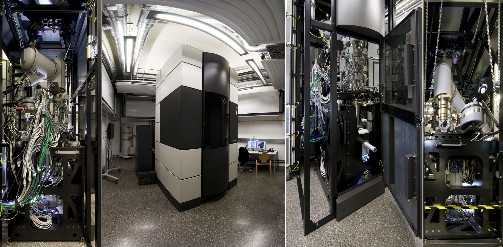
Transmission Electron Microscopes (TEM)
Transmission electron microscopy (TEM) and scanning transmission electron microscopy (STEM) are used to image the projected structure of thin, electron-transparent samples. Combined with a HAADF (high-angle annular dark-field) detectors, STEM can produce chemically sensitive images. The best possible resolution is in the range of 0.1 nm .A prerequisite for TEM investigations is that an electron-transparent sample can be prepared from the starting material. The maximum sample thickness that can be penetrated is in the order of 1000 nm. For high resolution TEM imaging, sample thicknesses below 50 nm are required. All necessary facilities including Focused Ion Beam (FIB) systems are available for preparation of material science samples. Biological thin sections can be prepared using an ultramicrotome. In diffraction mode, local diffraction images (fine range diffraction) can be acquired, which can be used to determine lattice plane spacing and crystal structures.
SEM/Focused-Ion-Beam (FIB) Combination
Scanning Electron Microscopes (SEM)
Scanning electron microscopy (SEM) is used to study the surface structure of samples in material science, nanotechnology, solid state physics, chemistry, process engineering, biology and geology. In most cases, no complex sample preparation is required. Electrically insulating objects must be vapor deposited with a thin carbon, gold or platinum film to avoid charging the sample in the microscope. Biological objects often need to be dried before examination.
Sample Holder
In the electron microscopes, different sample holders are used for various experiments.