
Transmission electron microscopy (TEM) and scanning transmission electron microscopy (STEM)
Transmission electron microscopy (TEM) and scanning transmission electron microscopy (STEM) are used to image the projected structure of thin, electron-transparent samples. Combined with a HAADF (high-angle annular dark-field) detector, STEM can produce chemically sensitive images. The best possible resolution is in the range of 0.1 nm.A prerequisite for TEM investigations is that an electron-transparent sample can be prepared from the starting material. The maximum sample thickness that can be penetrated is in the order of 1000 nm. For high resolution TEM images sample thicknesses below 50 nm are required. For the preparation of material science samples all necessary facilities including a Focused-Ion-Beam (FIB) system are available. Biological thin sections can be prepared using an ultramicrotome. In diffraction mode, local diffraction images (fine range diffraction) can be acquired, which can be used to determine lattice plane distances and crystal structures.
The TEM can be used in combination with analytical techniques (energy dispersive X-ray spectroscopy (EDXS), electron energy loss spectroscopy (EELS) and energy filtering TEM (EFTEM)) for chemical analyses, for the investigation of bonding and oxidation states as well as electronic properties.Using an electron beam focused to a small diameter, analytical studies can be performed with sub-nanometer resolution.
Electron holography in a transmission electron microscope allows the reconstruction of the wave function at the bottom of the sample. The phase of the wave function contains, among other things, information about internal and external electric and magnetic fields. Tomographic investigations provide information about the three-dimensional structure of nanoparticles, precipitates and pores.
Typical applications of TEM are:
- Characterization of defects (dislocations, stacking faults), determination of the distribution and density of defects.
- atomic structure of interfaces, nanoparticles, .....
- distribution and size of precipitates, particles and cavities
- analysis of different phases, representation of distribution of different elements
- grain boundary structure and segregation of foreign atoms in grain boundaries
- Imaging of internal nanoscale electric fields, e.g. at charged dislocations and grain boundary
Contact person:
Applications as well as the fee schedule for services can be found here.
Examples
Cross-sectional image of nanocrystalline (LaSr)CoO3 films on Y-doped ZrO2 and Gd-doped CeO2: color-coded distribution of La, Sr, Co, Zr
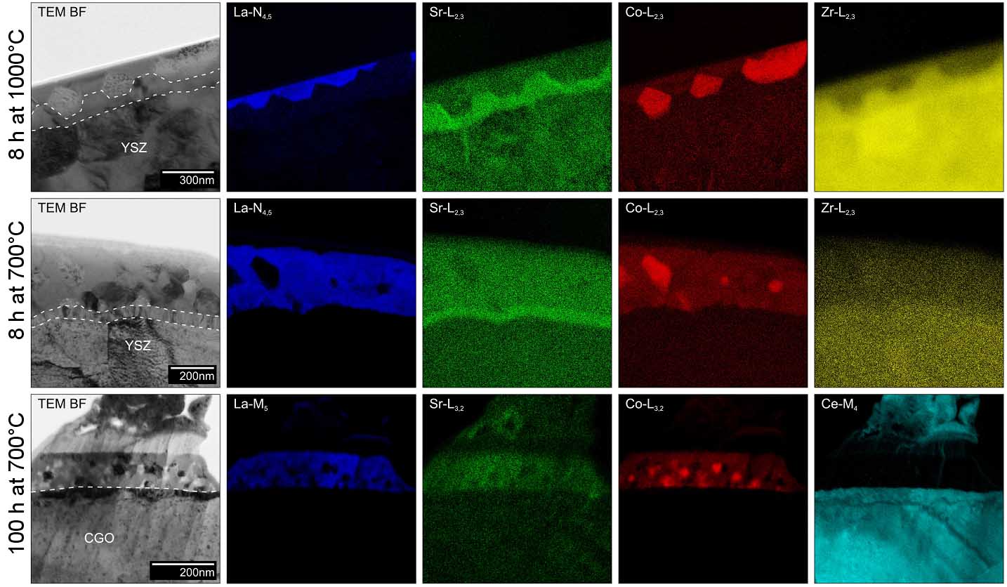
L. Dieterle et al, J. Mat. sci. 43, 3135 (2008)
Pt clusters on a thin amorphous carbon layer
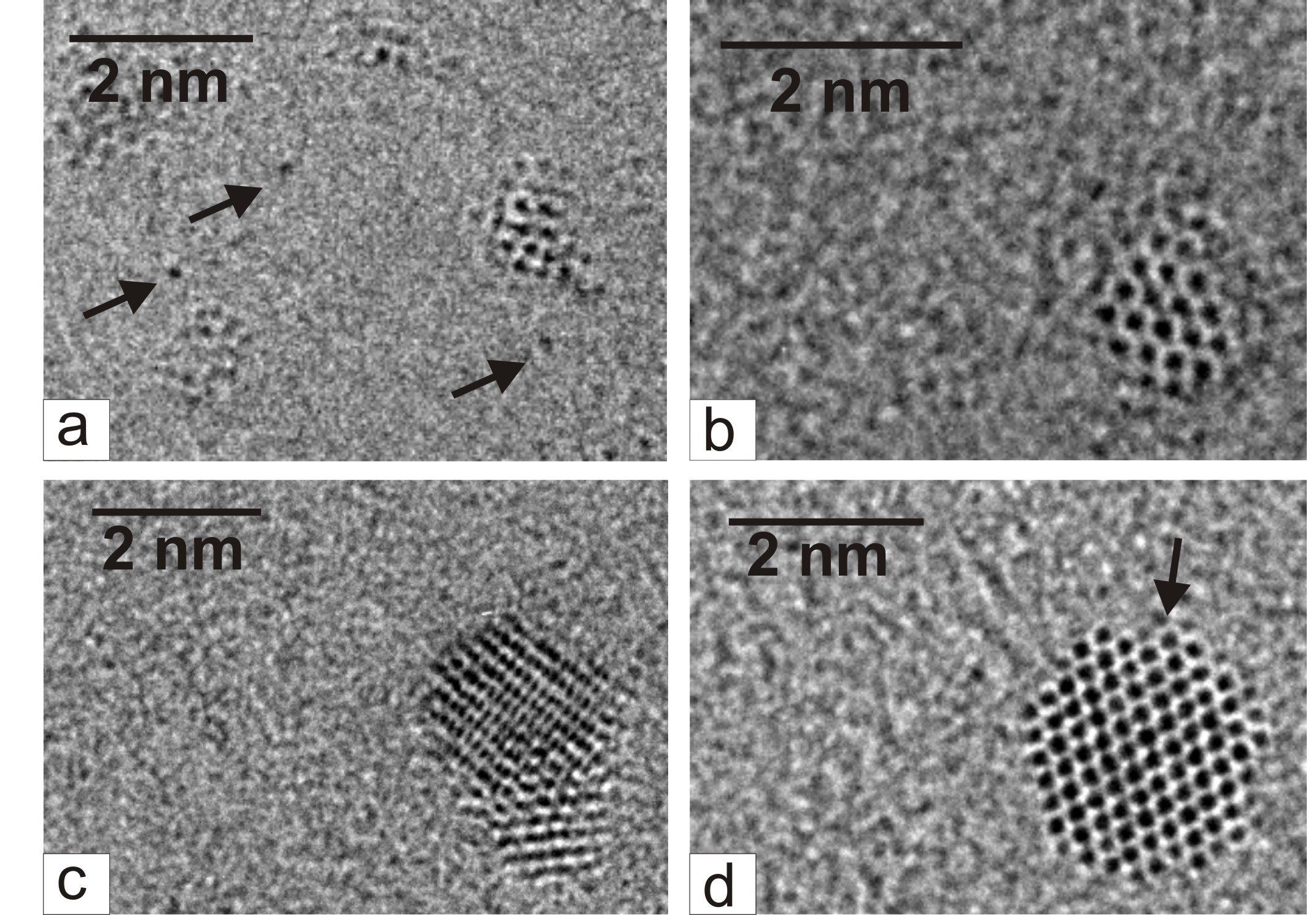
Reinhard Schneider, Holger Blank (Laboratory for Electron Microscopy)
Cross-sectional images of a Zn0.69Mn0.31Se/GaAs(001) semiconductor heterostructure: (a) diffraction image along the [110] zone axis with twin orientations (2,3) and (b) dark field image from the region of the diffraction image with imaging vector g=(220), (c) dark field image with g=(111).
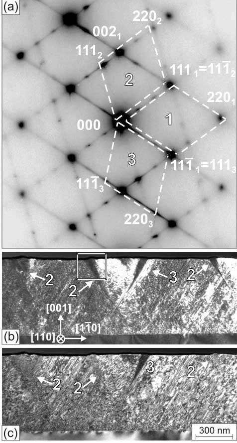
D. Litvinov et al, J. Appl. Phys.100, 023523 (2006).
Cross-sectional image of a GaAs/Si(001) semiconductor heterostructure: dislocations in an epitaxial GaAs layer on silicon substrate
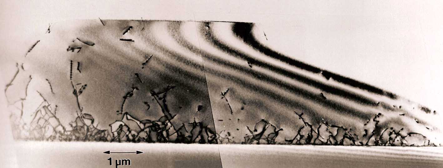
D. Gerthsen (Laboratory for Electron Microscopy)
Bacteria
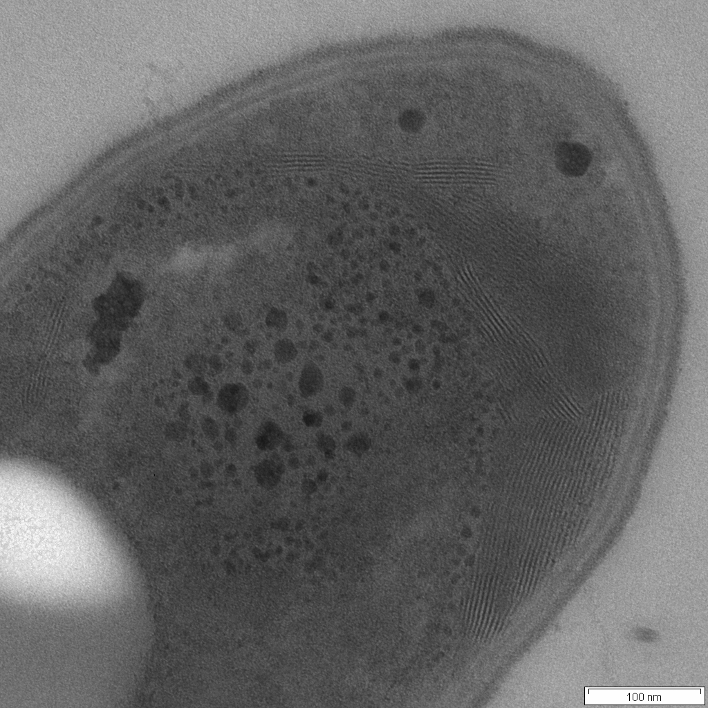
Dense packing lamellar oriented membrane structures and multiple electron dense inclusion bodies on apical part of bacterial cells of Aneurinibacillus migulanus DSM 5658, producing Gramicidin S. Ultrathin section of cells, taken during the transition to stationary growth phase, were done by Dr. Marina Berditsch (KIT, Institute of Organic Chemistry, Department Biochemistry) and TEM by M. Fotouhi (Laboratory for Electron Microscopy).