
3D Printed Functional Organic and Inorganic Materials and Devices
Nowadays, 3D printing or additive manufacturing has been applied to a variety range of materials, from polymers, metals to ceramics. Within the 3D Matter Made To Order (3DMM2O) cluster of excellence, our focus is to characterize and understand the local structure and functional properties of 3D printed organic and inorganic materials and devices. By employing the state-of-the-art analytical electron microscopy techniques in combination with in-situ and ex-situ stimuli, we aim to provide insights into these 3D printed metamaterials in atomic, nano and micro scales, facilitating the tailoring of novel materials and devices in a bottom-up manner.
In Situ Pyrolysis of 3D Printed Building Blocks of Functional Nanoscale Metamaterials
Contact: Qing Sun, Prof. Dr. Yolita Eggeler
3D nanolattice metamaterials have exceptional lightweight and unprecedented mechanical properties, which are derived from the geometry of their internal periodic structures rather than the properties of the constituent materials [1]. One promising way to fabricate 3D nanolattices is direct laser printing (DLW) of polymeric precursors based on two-photon polymerization (TPP) combining with a subsequent pyrolysis step [2]. The latter will introduce a great mass loss and volumetric shrinkage by outgassing when temperature goes up to around 400-600 °C for most polymers. However, a comprehensive and predictable shrinkage behavior is remaining to be studied.
In this work, we aim to systematically investigate the shrinkage dynamics of 3D printed microstruts by in situ environmental scanning electron microscopy (ESEM) heating. These 3D printed microstruts are used as building blocks for functional nanolattice metamaterials. As a novel approach for sample preparation, we directly print IP-Dip photoresist on Micro-electromechanical Systems (MEMS) based heating chip. The schematic is presented in Figure 1 [3].
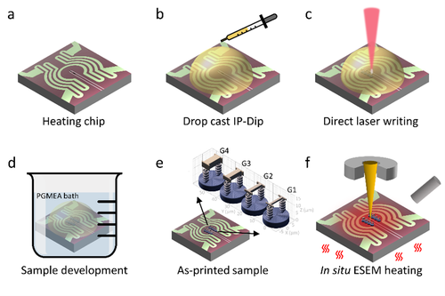
the micro-electro-mechanical systems (MEMS) chip by two-photon DLW
for in situ ESEM heating.
To correlate the effects of temperatures, atmospheric pressures as well as surface-to-volume ratios on isothermal shrinkage, we performed six in situ ESEM experiments at three temperature settings: 450, 500 and 550 °C, in two pressure regimes: high vacuum (HV) of 10−5 mbar and in a reduced nitrogen atmosphere of 3 mbar (LV), and on a series of microsturts with four different sizes: G1-G4. For the first time, the structural evolution of 3D printed structures is tracked continuously until a quasi-stationary state is reached (see Movie 1 [3]). The movie is generated by a stack of SEM images that are recorded continuously during the isothermal processes. Besides thermal dependence, i.e., the higher the temperature, the faster and greater the contraction, we observed the influence of environmental pressures. By tracking the strut length change, Figure 2a illustrates how the increased partial pressure (nitrogen atmosphere) altered the shrinkage behaviors.
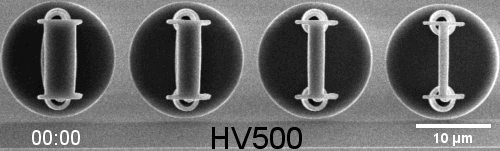
of IP-Dip microstruts in a high vacuum of 10−5 mbar at 500 °C.
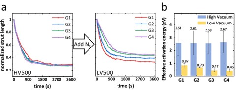
in high vacuum (HV) and low vacuum (LV) conditions. a) Pyrolysis kinetics
of in situ heating experiments at 500 °C for two different atmospheric regimes:
normalized length (projected) of each microstrut with respect to heating time
in one hour. b) The effective activation energies for the microstruts with
different cross-sections (G1– G4) in high and low vacuum conditions.
Furthermore, we investigate the cross-sections of these heated microstruts in an analytical transmission electron microscope (TEM) to get more insights into the diffusion/degassing process during pyrolysis. These cross-sections are prepared by focused ion beam (FIB) cutting. Scanning transmission electron microscopy (STEM) combined with electron energy loss spectroscopy (EELS) is a powerful characterization method that allows to measure not only atomic composition, but also chemical bonding with high spatial resolution. The carbon and oxygen mappings in Figure 3 confirm an additional oxygen enriched contour (oxygen outer ring) accumulated only around the surface of the samples that are pyrolyzed in nitrogen atmosphere (LV).
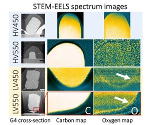
heating conditions by STEM-EELS. Left panel: Bright field (BF-) STEM images
of the cross-sections of microstrut G4 prepared by FIB cutting. Right panels:
Two columns of spectrum images showing the carbon (left) and oxygen (right)
distribution in the micorstruts cross-sections.
Besides SEM and TEM investigations, we performed model-free master curve approach [4] to calculate the effective activation energy Eaeff from these pyrolysis-induced shrinkage curves. Its results (Figure 2b) reveal that Eaeff is approximately four times larger under vacuum conditions than in a nitrogen atmosphere (2.6 eV vs. 0.5–0.9 eV, respectively). Additionally, this in situ experimental pyrolysis design can be extended to investigations of various other polymer precursors and additive manufacturing methods.
[1] Bauer, J., et al. (2017). "Nanolattices: An Emerging Class of Mechanical Metamaterials." Advanced Materials 29(40): 1701850.
[2] Eggeler, Y. M., et al. (2023). "A Review on 3D Architected Pyrolytic Carbon Produced by Additive Micro/Nanomanufacturing." Advanced Functional Material: 2302068.
[3] Sun, Q., et al. (2023). "In Situ Pyrolysis of 3D Printed Building Blocks for Functional Nanoscale Metamaterials." Advanced Functional Materials: 2302358.
[4] Niekiel, F., et al. (2015). "The process of solid-state dewetting of Au thin films studied by in situ scanning transmission electron microscopy." Acta Materialia 90: 118-132.
![]()
Electron microscopy to reveal internal structural properties of laser printed inorganic nanoarchitectures
Contact: Kristian Kraft, Prof. Dr. Yolita Eggeler
Newly developed printing techniques of metallic conductors and whole functional devices [1] have been established in recent years. The printing by laser or inkjet printer allows to create structures in the microscale. Printing such devices benefit from low production costs and high production speeds.
Electron microscopy is used to characterize these printed devices [2] on their micro- and nanoscale [4], as well as their electrical properties [3]. In situ scanning electron microscopy (SEM) allows electrical probing possibilities. With dual focused ion beam (FIB)-SEM the devices are prepared for investigations in transmission electron microscopes (TEM) in order to analyze their local chemical compositions and bonding states using scanning transmission electron microscopy ((S)TEM) and high-resolution transmission electron microscopy (HRTEM) in combination with spectroscopy such as energy-dispersive x-ray spectroscopy (EDXS) and electron energy loss spectroscopy (EELS).
Such devices under investigation are memristors (shown in Figure 4a). Memristors are characterized by the fact that their resistance depends on the voltage that was applied to the component in the past. By applying a positive voltage on the silver electrode and ground on the platinum electrode, a conductive filament is formed in the zinc oxide between the two electrodes (shown in Figure 4b). FIB-SEM tomography is performed to fully describe the Ag distribution in memristors that have experienced electrical characterization (cycled memristor) and non-cycled memristors. For tomography, a protective Pt layer is deposited on the memristor (Figure 5) and a trench is cut in front. From above, slice by slice is removed with the FIB and under an angle with the SEM the region of interest (ROI) is imaged. The reconstructed 3D movies from the 2D images are shown in Movie 2a for the cycled and in Movie 2b for the non-cycled memristor. An important finding is that due to the electrical characterization Ag (in green) accumulates around the lower Pt electrode. In further 3D reconstruction experiments, the aim is to map the conductive Ag filaments responsible for the conduction mechanism.
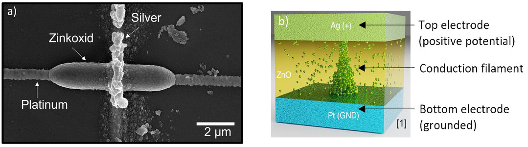
and the Pt. b) Scheme of conductive Ag filament in the ZnO. Here, a ground potential is applied to Pt and a positive potential is applied to Ag top electrode
for the forming process.
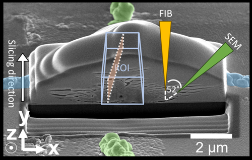
is marked in blue and the Pt electrode in green. The ZnO is located under the
protective Pt layer. 3D reconstruction is performed from the ROI. With the FIB, slices
are removed from the top and the SEM images are taken at an 52° angle.
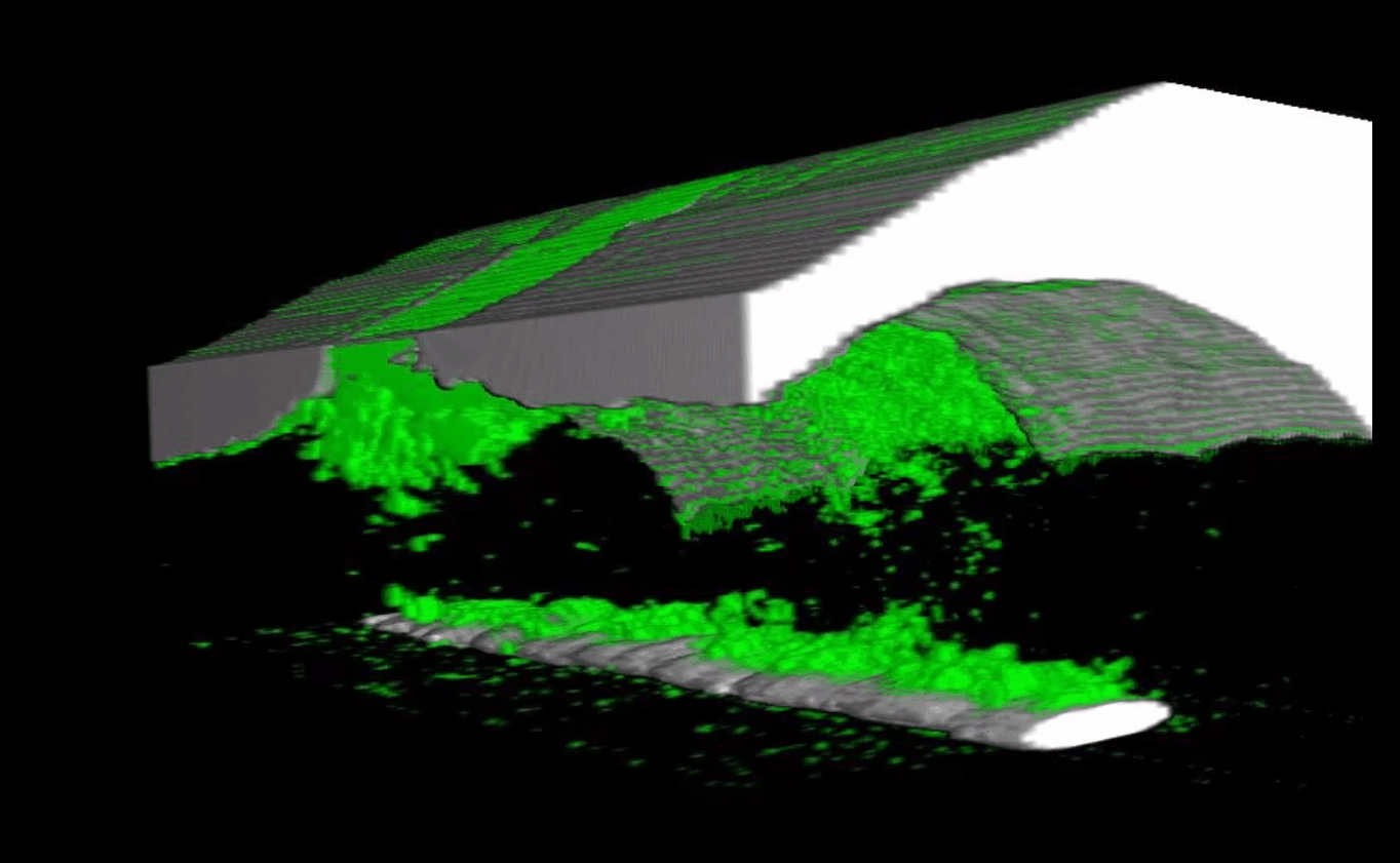
The Ag is shown in green and Pt in white.
Ag is distributed at Pt bottom only for the
cycled memristor. The Ag top electrode
is located under the protective Pt layer.
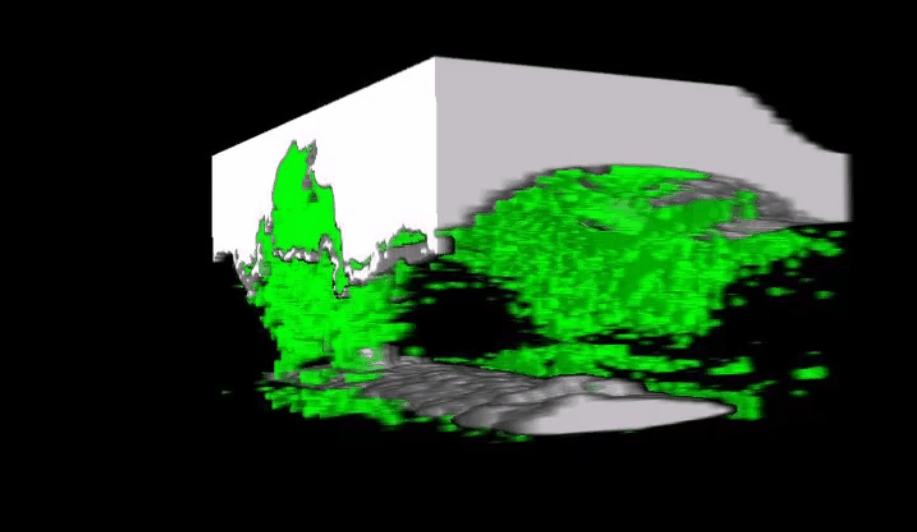
The Ag is shown in green and Pt in white.
Ag is distributed at Pt bottom only for the
cycled memristor. The Ag top electrode
is located under the protective Pt layer.
The aim of a further investigations is to gain a deeper understanding of the scaling parameters on the performance of the printed conductive devices and the formation and conduction mechanisms in the structures [5]. Furthermore, the influence of crystallinity, orientations and internal defects on the printed metallic structures is investigated. Diffraction techniques such as electron backscatter diffraction (EBSD) is used for this purpose. The special feature of the EBSD experiments is that the printed structures are polished with the FIB on the micrometer scale and at a very high angle. Here, printed ZnO single crystals are examined, in which a rotation of the crystal can be observed.
Another research area is dedicated to the development of a lateral memristor design in which material changes are visualized and the resulting switching mechanism [6] by external electrical stimulation in in situ SEM is observed. The aim is to observe in situ the formation of a conductive filament in a memristor.
References
[1] Yang, L., et al. (2023). "Laser Printed Microelectronics." Nature Communications 14(1): 1103.
[2] Hu, H., et al. (2023). "A Fully Inkjet-Printed Unipolar Metal Oxide Memristor for Nonvolatile Memory in Printed Electronics." IEEE Transactions on Electron Devices 70 (6): 3051–3056.
[3] Hu, H., et al. (2021). "Inkjet- Printed Bipolar Resistive Switching Device Based on Ag/ZnO/Au Structure." Appl. Phys. Lett. 119(11): 112103.
[4] Sun, Q. et al. (2023). "In Situ Pyrolysis of 3D Printed Building Blocks for Functional Nanoscale Metamaterials." Advanced Functional Materials: 2302358.
[5] Hu, H. et al. (2023). "Inkjet-Printed Tungsten Oxide Memristor Displaying Non-Volatile Memory and Neuromorphic Properties." Advanced Functional Materials: 2302290.
[6] Yi, H. et al. (2020). "Coexistence of Digital and Analog Resistive Switching Behaviours in Ag/CuAlO2/TiO2/P++-Si Memristor." Journal of Physics Conference Series: 1637(1): 012053.