Our research activities are in the following areas:
Application of electron microscopy to scientific questions in solid state physics, materials research, nanotechnology and biology
Method development in electron microscopy
Electron optics
Nanostructuring
News
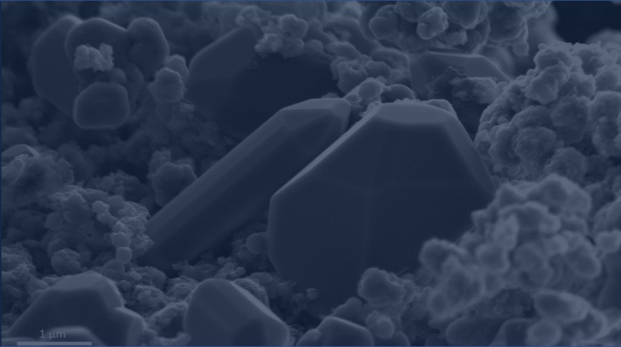
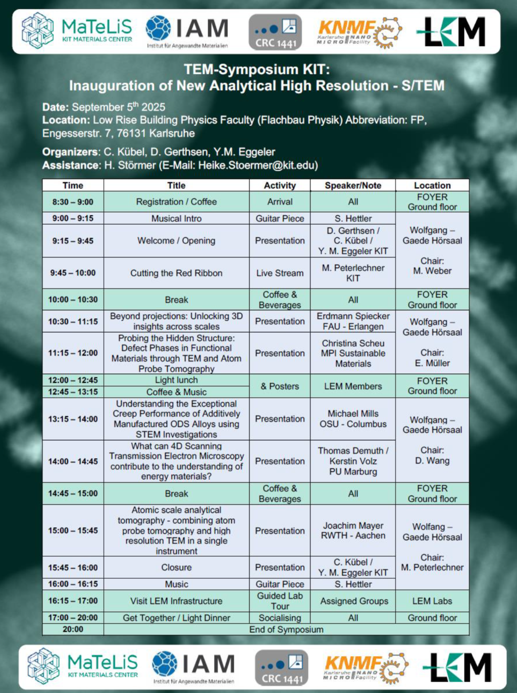
Inauguration Symposium für unser neues TEM
Highlight des Jahres: Unser TEM Symposium! Danke an die eingeladenen Sprecher für ihre fantastischen Vorträge! Danke für die vielen Posterbeiträge zu den begeisternden Forschungsthemen und danke an alle, die bei der Organisation geholfen haben!
Highlight of the year: Our TEM Symposium! Thanks to the invited speakers for their fantastic talks! Thanks to the poster presenters for sharing their exciting research and thanks to everyone for joining and helping organize it.
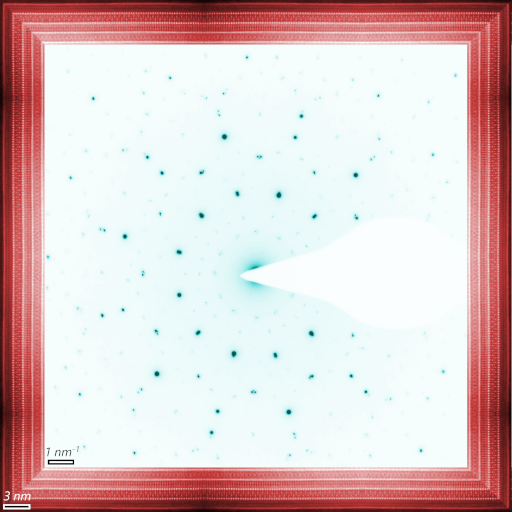
Dr. Simon Hettler receives the award “Best Image in Materials” for his contribution entitled “Misfit (a)symmetry” at the Microscopy at the frontiers of science (MFS) conference 2025 held in Valencia.
Selected-area electron diffraction (SAED) pattern of a flake of the misfit layered compound (MLC) SmS-TaS2 framed by a high-resolution scanning transmission electron microscopy (HRSTEM) image taken from a nanotube made of the MLC LaS-TaS2. MLCs are made up of two slabs of different materials (e.g. TaS2 and SmS or LaS), which are stacked alternatively. Due to the lattice mismatch between the two subsystems, the compound is incommensurate. The two slabs are revealed in the HRSTEM image frame and the complex interplay between the hexagonal TaS2 and the rocksalt lattice of SmS are reflected by the multitude of spots in the SAED pattern.
From September 1 to 4, 2025, the Electron Microscopy Conference in Karlsruhe (MC2025) will take place – and the LEM at KIT will be particularly well represented this year.
Our contributions at a glance: 2 workshops, 3 oral presentations, and 14 poster presentations.
We look forward to presenting our latest research results and developments and to engaging in discussions with the scientific community.
Visit us at the conference – we look forward to the exchange!
Stop by our shop window at Kaiserstraße 143 in Karlsruhe and discover the hidden world of mint, thyme & more – captured in stunning detail with the electron microscope.
ART | SUMMER | TECHNOLOGY – surprising, inspiring, free of charge.
At the KIT Study Info Day, Simon Hettler from the Laboratory for Electron Microscopy and Phillip Willke from the Physics Institute (PHI) gave a talk on "Quantum Physics in Your Smartphone."
They explained how quantum effects like tunneling and semiconductor physics shape everyday technology — in smartphones, cameras, and memory chips.
A key focus was on electron microscopy, which makes nanostructures visible and helps us better understand quantum physics.
Thanks to everyone who joined and showed interest! We look forward to seeing you again at KIT.
Open Day Highlight: Hands-on Microscopy for Kids!
As part of our Open House celebrating 200 years of KIT, one of the most beloved stations was our hands-on light microscopy activity for children.
Young visitors became scientists for a day – exploring flowers and insects under the microscope and proudly taking home their very own "microscopy certificate".
It was a fantastic day filled with curiosity, discovery, and joyful learning – for kids and adults alike.
A big thank you to everyone who joined us – we loved sharing the wonders of microscopy with you and hope to see you again soon!