
Focused Ion Beam (FIB) microscopy and nanostructuring
The combination of a scanning electron microscope with an ion-optical column, which generates a focused Ga+ ion beam, opens up a variety of new options for the analysis of microstructure and chemical composition. In particular, the 30 keV Ga+ ions allow us to "mill" nanostructures. Our dual-beam FIB/REM system type FEI Strata 400 STEM is additionally equipped with an EDXS system for chemical analyses and a detector for scanning transmission electron microscopy (STEM) for the investigation of electron-transparent samples. Due to the good spatial resolution of better than 1 nm for STEM images, the examination of samples in a transmission electron microscope may be unnecessary. A gas injection system allows local deposition of platinum, tungsten, SiO2 and carbon.
Additional options in addition to scanning electron microscopy (SEM)
- Micro- and nanostructuring by "milling" with the focused Ga+ ion beam
- Fabrication of cross sections and electron transparent samples for (scanning) transmission electron microscopy (TEM) and STEM, target preparation, small amount of material required
- STEM imaging at low electron energies <= 30 keV for the investigation of radiation sensitive objects (no displacement damage) with a resolution better than 1 nm
- Chemical sensitive imaging (qualitative) by HAADF (high-angle annular dark-field) STEM with a resolution of 1 nm
- EDXS analysis with high spatial resolution in the range of several nanometers (depending on sample thickness) on thin TEM samples
- Ion-induced channeling contrast for imaging of grain structure
- electrical contacting of nanoscale objects by local ion- and electron-induced Pt- or W-deposition
Contact person:
Applications as well as the fee schedule for services can be found here.
Examples
Ion induced channeling contrast of the grain structure on a cross section of a pearlitic steel after surface treatment
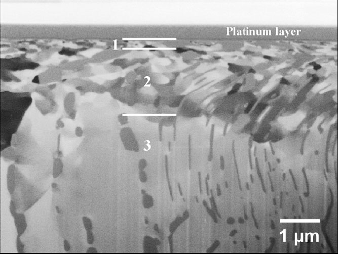
B. Okolo et al., Journal of Materials Processing Technology 183 (2007) 160-164 Target preparation of a TEM sample with in-situ liftout
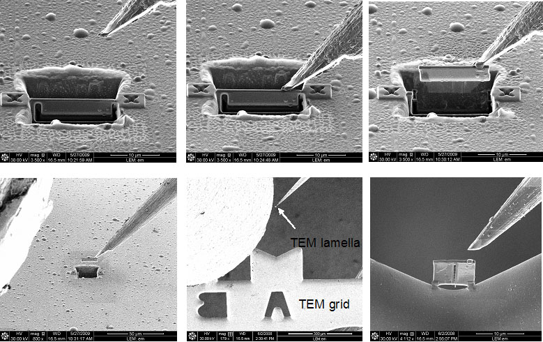 E.
E.
Müller (Nanostructure Service Laboratory of the Center for Functional Nanostructures CFN, KIT)
Electrical contacting of a ZnO nanopillar by local Pt deposition
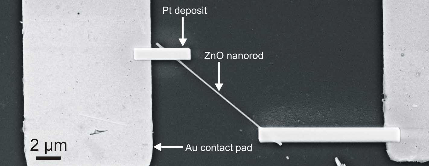
D. Weissenberger (Laboratory for Electron Microscopy)
30 keV HAADF (high-angle annular dark-field) STEM image of a HT-29 cell with incorporated SiO2 nanoparticles without contrasting
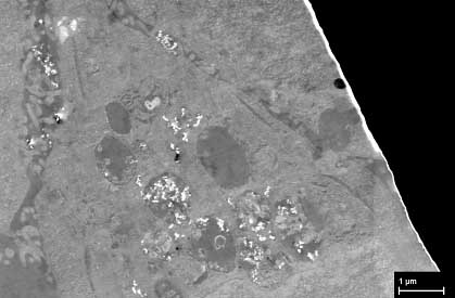 H. Blank
(Laboratory for Electron Microscopy), sample from the group of Prof. Dr. Doris Marko (Institute for Analytical Chemistry and Food Chemistry, University of Vienna)