
Quantification and Mitigation of Electron-Beam-Induced Carbon Contamination
Electron-beam induced carbon contamination is an unwanted side-effect of almost all electron microscopy investigations. Contamination results from electron-beam-induced polymerization of carbon-rich organic molecules on the sample surface, which can be either already present from sample preparation or from adsorption of molecules from the residual gas atmosphere in the microscope [1]. The growth of contamination is unwanted since it covers structures of interest and worsens the lateral resolution. Contamination processes are of special interest for typical SEM energies (≤ 30 keV), where contamination is particularly pronounced. This work aims to quantitatively measure contamination thicknesses and understand the factors that determine electron-beam-induced carbon contamination. The gained knowledge is applied to determine effective cleaning methods.
Although contamination is a daily issue, only a few systematic experimental studies about growth mechanisms and methods of contamination mitigation are available [2-5]. In addition, an approach exists to model electron-beam-induced contamination in an electron microscope [6], which we use for comparison with experimental data. Our experimental STEM‑in‑SEM setup allows analyzing contamination systematically and quantitatively. Relevant parameters (electron energy, beam current, dwell time, and others) are studied regarding their influence on contamination. Besides understanding the basic mechanisms of contamination growth, different contamination mitigation strategies are tested.
In this work, contamination patterns were grown in Thermo Fisher Helios G4 FX and FEI DualBeam Strata 400S dual-beam instruments at electron energies between 0.35 and 30 keV. Thin amorphous carbon films (~10 nm) were mainly used as substrates. They were prepared by carbon thread evaporation and were transferred to standard Cu TEM grids. Alternatively, commercial Au, Pd, and Si3N4 films were used to examine the influence of the support material. Contamination was studied by setting up an electron-beam pattern of 3x3 squares with an area of 1 µm2 each. The total dose was controlled by varying the irradiation time of the square between 5 s and 10 min (Figure 1a). Reproducibility of the sample state and microscope setup was checked before any contamination tests by a reference measurement under the same conditions (20 keV and 50 pA electron-beam current).
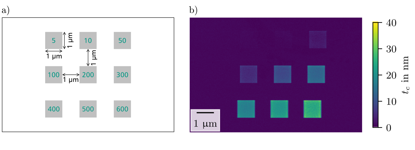
Figure 1. a) Pattern for electron-beam-induced contamination with numbers in the squares indicating the scan time in seconds. b) Color-coded thickness map of contamination grown at 20 keV on an amorphous carbon film. The thickness of the support film is subtracted.
We analyzed the contamination thickness by quantification of high-angle annular dark-field scanning transmission electron microscopy (HAADF-STEM) images, acquired after the contamination tests in the same microscope. The local sample thickness was quantified by normalizing the HAADF-STEM intensities with respect to the intensity of the primary electron beam and comparison with normalized intensities calculated by Monte-Carlo simulations. This quantification technique enables fast and reliable determination of local sample thicknesses if the sample and microscope properties are well known. A resulting contamination thickness map is shown in Figure 1b. Averaging the thickness in each square yields average contamination thicknesses tc as a function of the irradiation time (Figure 2a). The contamination thickness increases with scanning duration without showing saturation in the investigated time range. Even for longer irradiation times (up to 140 min), we found that the contamination continues to grow.
Figure 2a also shows that tc increases with decreasing electron energy, as expected because of the increased interaction between the specimen and the electron beam at lower energies. The results of such measurements allow us to derive strategies for a practical reduction of contamination by choosing the image-acquisition parameters carefully. Other experiments demonstrate, e.g., that contamination is reduced for a specific dose applied in a short time rather than in a long time. Also, a shorter dwell time in STEM leads to preferential contamination at the edges of the scanned region and reduces contamination in the center.
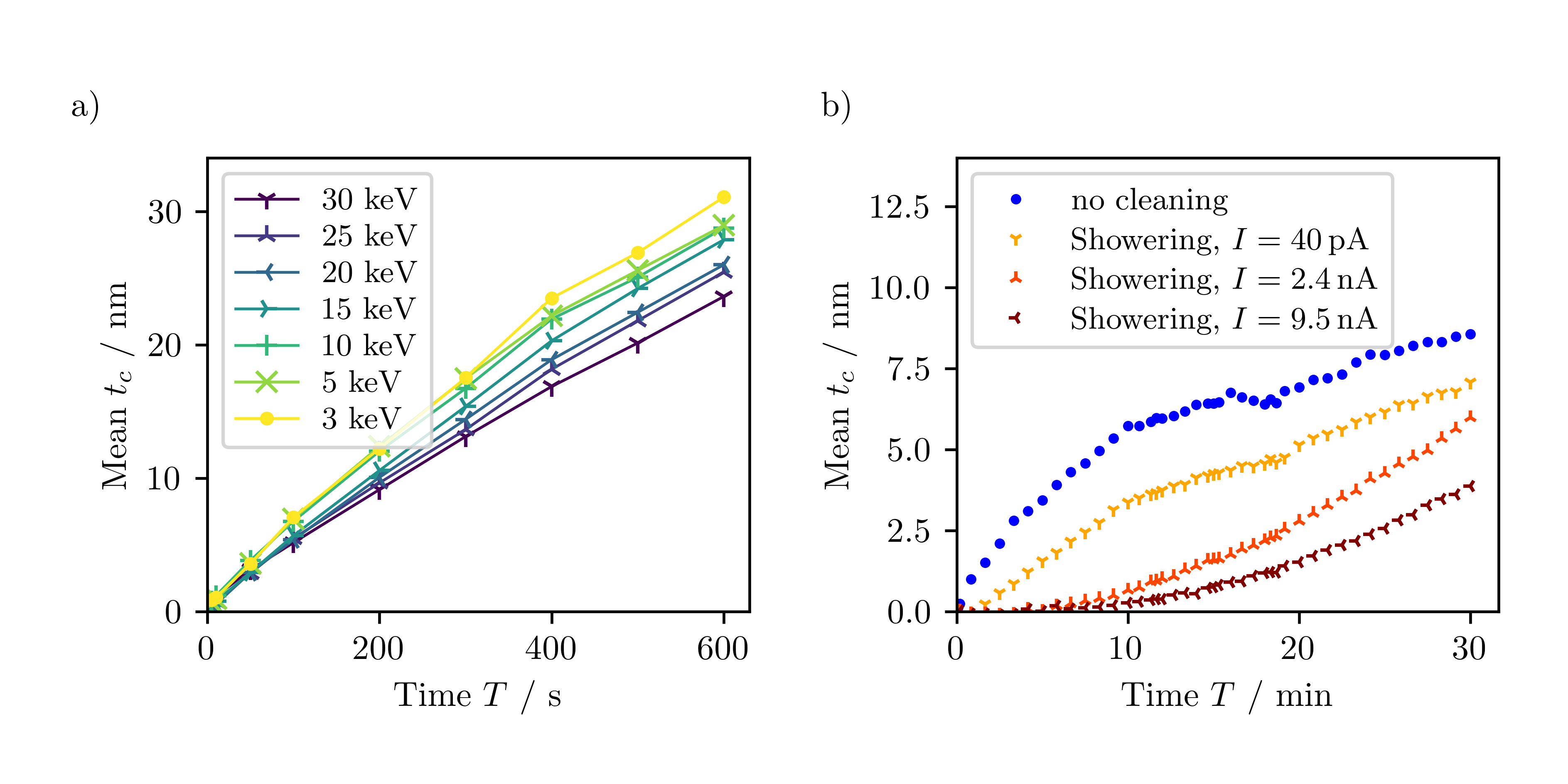
Figure 2. a) Contamination thickness as a function of the scanning time T for different electron energies. b) Beam showering test at 20 keV. After beam showering a 40x40 mm2 region with different beam currents (see legend) for 10 min, the contamination thickness tc of a small 1x1 mm2 patch in the center of the showered region is plotted as a function of the scanning time up to 30 min. The blue data was obtained without beam showering.
Sample treatments like cooling, baking, plasma cleaning, and beam showering are expected to reduce contamination and were tested by Mitchell at 200 keV [5]. In our study, sample treatments are tested at energies ≤ 30 keV. We focus on methods that do not require cooling because cooling stages are rarely available in scanning electron microscopes. Figure 2b presents the results of beam showering. Beam showering was performed by scanning regions with a size of 40 x 40 µm2 for 10 min with beam currents between 40 pA and 9.5 nA before contaminating a 1 x 1 µm2 square (contamination patch) for 30 min in the center of the showered region. Figure 2b shows the measured contamination thickness of the contamination patches as a function of the scanning time compared to the contamination without beam showering (blue curve). The contamination growth is strongly reduced with the most pronounced effect for the highest showering electron current. Nevertheless, contamination is not completely suppressed but increases with scanning time. This can be explained by contaminants from outside the showered area that can reach the contamination patch by diffusion after some time. Beam showering is thus very effective but does not permanently prevent contamination.
In sum, our technique for measuring beam-induced carbon contamination is well-suited to quantitatively investigate contamination growth and test sample cleaning methods. Practical instructions for mitigation of contamination are derived from those results.
References
[1] Reimer, Scanning Electron Microscopy Vol. 45, Springer (1998)
[2] Hirsch et al., Scanning 16, 101 (1993)
[3] Hettler et al., Micron 96, 38 (2017)
[4] Egerton, Micron 119, 72 (2019)
[5] Mitchell, Micron 73, 36 (2015)
[6] Müller, Optik 33, 296 (1971)
[7] We acknowledge funding by the Deutsche Forschungsgemeinschaft (DFG, German Research Foundation) under Germany’s Excellence Strategy – 2082/1 – 390761711 and thank the Carl Zeiss Foundation for financial support.