
The direct conversion of solar radiation into electrical energy is expected to cover a major fraction of the electricity supply in the upcoming decades. Therefore, novels materials, devices and methods are required for efficient future solar cells.
Kerasolar - Ferroelectric solar cells
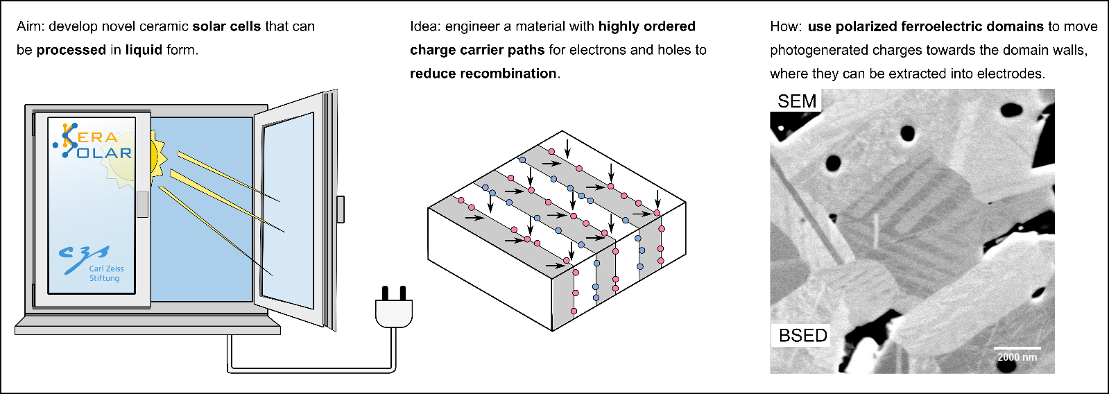
The Kerasolar project is working on a fundamentally new solar cell concept: ferroelectric solar cells. The ferroelectric polarization in semiconducting (oxide) ceramics separates the photogenerated charge carriers in the solar cell spatially and dissipates them along separate paths to the electrodes. This spatial separation minimizes the recombination of charges and increases efficiency. For the first time, the project combines photovoltaic research and research on functional ceramic materials.
The new technology marks a breakthrough in photovoltaic research by bringing together the most important advantages of other solar cell concepts: the printability of organic solar cells, the ferroelectricity of lead halide perovskites, and the long-term stability of silicon solar cells. The high variability of oxide ceramics also enables important optoelectronic properties such as bandgap or charge carrier mobility to be tailored. In the future, this new material class of ferroelectric semiconductor ceramics can also be used for other optoelectronic components such as LEDs, photodetectors, or transistors, which creates an extensive new field of research.
Eleven research groups from electrical engineering, functional ceramic materials, physics, and chemistry are working together in material selection, synthesis, characterization, and material processing to develop the perfect solar cell.
Our role in Kerasolar is to use analytical transmissions electron microscopy to characterize the selected synthesized materials. Only the transmission electron microscope techniques enable us to understand these new solar cell materials' complex physical and chemical properties.
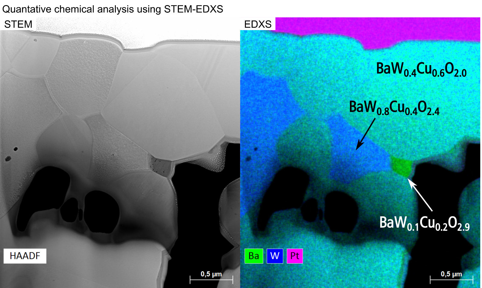
The main reason for this is the combination of sample imaging in real space, diffraction in reciprocal space, and chemical analysis with simultaneously high spatial resolution. Transmission electron microscopy (TEM) and scanning transmission electron microscopy (STEM) enables a detailed investigation of the structural properties, particularly critical for solar cell materials. Here, the size and orientation of the ferroelectric domains and the chemical homogeneity are crucial for the quality of the material.
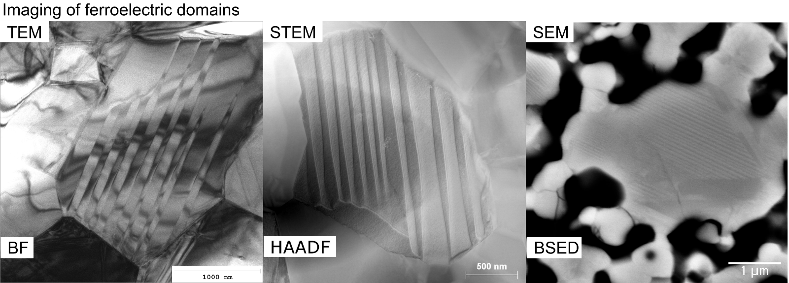
Fine-area diffraction images (SAED: selected area electron diffraction) and high-resolution TEM (HRTEM) images can be evaluated to examine the crystal structure of the solar cell materials. Furthermore, the chemical composition can be analyzed with spatial resolution using energy-dispersive X-ray spectroscopy (EDXS) in STEM mode. Here, element distribution images are generated, which can be used to determine variation in chemical composition within the solar cell and the differentiation of foreign phases or contamination.
Methodologically, however, the analysis is less suitable for light elements such as oxygen. Electron Energy Loss Spectroscopy (EELS) can be very helpful here, as ionization edges of light elements can be acquired with a high energy resolution. Due to this high energy resolution, EELS further provides information on chemical bonding, oxidation states, coordination changes, and short-range order.
Copper Indium Gallium DiSelenide (CIGS) Solar Cells
In recent years researchers have paid much attention to Cu(In,Ga)Se2 (CIGS) thin-film solar cells with Zn(O,S) buffer layers due to their high photovoltaic conversion efficiency [1] and non-toxic buffer layers. The solar-cell efficiency is significantly influenced by the chemical composition of each layer in the device, particularly the CIGS absorber and the Zn(O,S) buffer. Thus, it is of great importance to determine accurately the local stoichiometry of these layers in the final device. Scanning transmission electron microscopy (STEM) combined with energy-dispersive X-ray spectroscopy (EDXS) is a powerful technique for quantitative analysis of the local chemical composition with high spatial resolution. However, even for thin TEM specimens the accuracy of quantitative STEM/EDXS composition analyses can be severely affected by X-ray absorption and other effects. X-ray absorption is particularly influenced by the composition and local thickness of the TEM specimen, and these two parameters are generally unknown. Due to significant quantification errors for EDXS analyses of CIGS solar cells only intensities of X-ray lines are usually given in the literature [2, 3].
In this work, the influence of the local sample thickness on quantitative STEM/EDXS was studied for CIGS solar cells with Zn(O,S) buffer layers and ZnO:Al window layers. For this purpose, a multi-layer stack of sputtered Zn0.5O0.5 / Zn0.5O0.35S0.15 / Zn0.5O0.25S0.25 / Zn0.5O0.2S0.3 / Zn0.5S0.5 layers on a Si wafer was utilized as a reference in addition to the CIGS solar cells. Cross-sectional TEM lamellae with homogeneous thickness and wedge-shape specimens were prepared from the Zn(O,S) multilayers and solar-cell stacks, respectively, by focused ion beam (FIB) milling with a Thermo Fisher dual-beam Helios G4 FX microscope. To avoid the influence of Cu stray X-rays on EDXS quantification results, it is important to attach CIGS lamellae to Cu-free lift-out grids during FIB preparation of TEM lamellae. STEM imaging and EDXS analyses were performed using a FEI Tecnai Osiris microscope operated at 200 kV, which is equipped with a SuperX EDXS detector system comprising four Si-drift detectors. Quantification of the EDXS raw data was carried out by the Bruker Esprit software version 2.1 using the thin-foil approximation [4].
Figure 1a shows a cross-section high-angle annular dark-field (HAADF) STEM image of the Zn(O,S) multilayer stack on Si where the nominal S/O concentration ratio increases from the bottom layer to the top layer. An element-concentration profile (see Figure 1b) of the region marked by an arrow was obtained by applying the thin-foil approximation for the evaluation of the EDXS data. The determined S concentration in each layer agrees well with the nominal value, while the O concentration is lower and the Zn concentration is higher than the correct stoichiometry owing to the thickness-dependent absorption of the low-energy O-Kα X-rays. X-ray absorption of oxygen was taken into account in the composition profile shown in Figure 1c. The lamella thickness was adapted to obtain the correct stoichiometry for ZnO with known composition and a ZnO material density of 5.61 g/cm3. The absorption-corrected composition profile in Figure 1c shows that the measured composition of each layer is consistent with its nominal value within an error limit of ± 2 at.%. This indicates that the X-ray absorption in Zn(O,S) layers with different S/O concentration ratios can be properly taken into account by the absorption correction on the basis of the ZnO layer, if the local thickness does not significantly change. Furthermore, it can be deduced that in a multilayer system including a ZnO layer as in CIGS solar cells, the X-ray absorption of oxygen in all the O-containing layers can be corrected by the use of the ZnO layer. On the contrary, the thickness-dependent absorption of O X-rays can be exploited to determine the local thickness of the TEM sample. In addition, the correct stoichiometry of the Zn(O,S) layers can also be achieved by an iterative method.
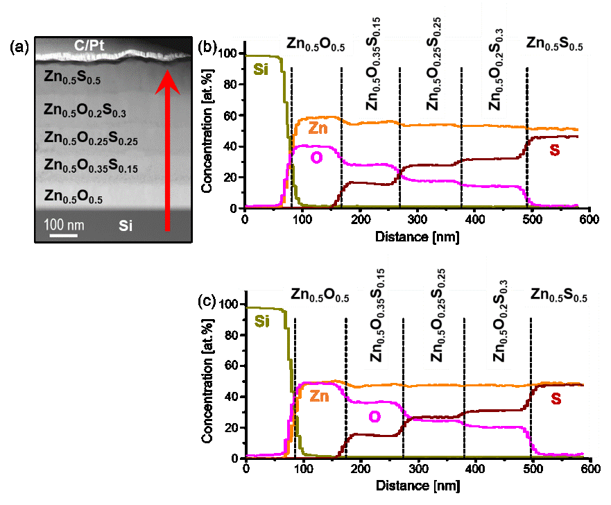
Figure 1. (a) Cross-section HAADF STEM image of a stack of sputtered Zn(O,S) layers with different S/O concentration ratios on a Si substrate coated with a carbon and platinum layer on top. An EDXS line profile was acquired along the arrow. The element concentrations of the quantified EDXS line profiles are shown in (b) without and (c) with absorption correction.
Figure 2a shows a top-view secondary-electron scanning electron microscopy (SE-SEM) image of a wedge-shaped TEM sample of the CIGS solar cell, which shows a wedge angle of 25˚. A cross-section HAADF STEM image of this wedge-shaped sample is depicted in Figure 2b, where the local sample thickness is well known as a function of the distances from the thin wedge edge. The thickness-dependent quantified EDXS line profile along the arrow is shown in Figure 2c. In thick regions (> 100 nm), the evaluated concentration of each element agrees well with the integral chemical composition of Cu(In0.7Ga0.3)Se2 (i.e. 24 at.% Cu, 18 at.% In, 8 at.% Ga, 50 at.% Se) as determined by X-ray fluorescence. However, in thin regions (< 100 nm) the determined Se concentration is much lower, the In slightly lower, and the Cu much higher than the nominal value. This artifact may result from a preferred Se and In evaporation compared to that of Cu and Ga during ion-beam milling [5], likely to be related to the different vapor pressures of these elements (Se > In > Ga > Cu) in CIGS, which in practice cannot completely be prevented. Besides, the existence of O indicates the oxidation of the TEM lamella. The influence of element evaporation and sample oxidation is more pronounced in thin regions, because these effects generally occur at the sample surface. Thus, it is important to use lower ion-beam energy and smaller ion currents, and to keep the sample temperature for FIB milling as low as possible by using sample cooling stage. Also, the TEM sample should be stored under O-free conditions.
Figure 2. (a) Top-view SE-SEM image and (b) cross-section HAADF STEM image of a wedge-shaped TEM lamella of a CIGS solar cell. (c) Quantified EDXS line profile of the CIGS layer obtained as a function of the local sample thickness along the red arrow in (b).
References
[1] M. Nakamura, K. Yamaguchi, Y. Kimoto, Y. Yasaki, T. Kato, H. Sugimoto, Cd-free Cu(In,Ga)(Se,S)2 thin-film solar cell with record efficiency of 23.35%, IEEE J. Photovolt. 9 (2019) 1863.
[2] M. Kim, J. Lee, Y. Lee, J.H. Jeong, K.B. Lee, Structural and compositional analyses of Cu(In,Ga)Se2 thin film solar cells with different cell performances, J. Vac. Sci. Technol. B 34 (2016) 03H121.
[3] J.S. Wu, A.M. Kim, R. Bleher, B.D. Myers, R.G. Marvin, H. Inada, K. Nakamura, X.F. Zhang, E. Roth, S.Y. Li, T.K. Woodruff, T.V. O'Halloran, V.P. Dravid, Imaging and elemental mapping of biological specimens with a dual-EDS dedicated scanning transmission electron microscope, Ultramicroscopy 128 (2013) 24.
[4] G. Cliff, G.W. Lorimer, The quantitative analysis of thin specimens, J. Microsc. 103 (1975) 203.
[5] Y. Yan, K.M. Jones, R. Noufi, M.M. Al-Jassim, Argon ion beam and electron beam-induced damage in Cu(In,Ga)Se2 thin films, Thin Solid Films 515 (2007) 4681.
[6] We acknowledge funding by the German Federal Ministry for Economic Affairs and Energy (BMWi) within the EFFCIS-II project under contract No. 03EE1059A (ZSW) and contract No. 03EE1059E (KIT).
Finished: Organic Solar Cells
Organische Solarzellen bieten im Vergleich zu den traditionellen auf Silizium basierenden Solarzellen viele neuartige technologische Möglichkeiten. Die größten Vorteile sind hierbei wohl die geringen Herstellungskosten, die geringere Umweltbelastung und die mechanische Flexibilität. Diese Eigenschaften eröffnen ein Feld völlig neuer Anwendungsmöglichkeiten.
Der Schwerpunkt der Forschung liegt momentan zum einen auf der Verbesserung der Effizienz der Solarzellen, welche zurzeit bei 8,3% (Konarka Inc.) liegt, zum anderen auf der Verlängerung der Lebensdauer.
Unsere Forschung richtet sich auf die Morphologie der Absorber-Schicht, die mit verschiedenen mikroskopischen Techniken untersucht wird. Die untersuchten Solarzellen werden hergestellt von der Arbeitsgruppe von U. Lemmer (Lichttechnisches Institut, KIT).

Die Absorberschicht enthält zwei organische Halbleitermaterialien: als Akzeptor das Fulleren-Derivat PCBM und als Donator-Material P3HT (Poly(3-Hexylthiophen)). Der Grad der Entmischung dieser beiden Stoffe ist ausschlaggebend für die Leistung der Solarzelle, da die Exzitonen, die durch die einfallenden Photonen gebildet werden, aufgrund ihrer hohen Bindungsenergie nur an der Grenzfläche zwischen Donator und Akzeptor getrennt werden können. Auf der anderen Seite müssen die beiden unterschiedlichen Polymer-Phasen groß genug sein, damit der Ladungstransport zu den Elektroden gewährleistet ist. In der Abbildung links ist eine vereinfachte Abbildung einer organischen Solarzelle mit Phasenseparation in der Absorberschicht zu sehen.
Bis jetzt gibt es wenige zufriedenstellende Methoden um die verschiedenen Phasen in der photoaktiven Schicht abzubilden. Dies liegt daran, dass die mittleren Ordnungszahlen und die Dichten der beiden Materialien sehr ähnlich sind und es sich bei beiden Stoffen um schwach streuende Materialien handelt. Dazu kommt noch dass beide Materialien sehr strahlungsempfindlich sind.
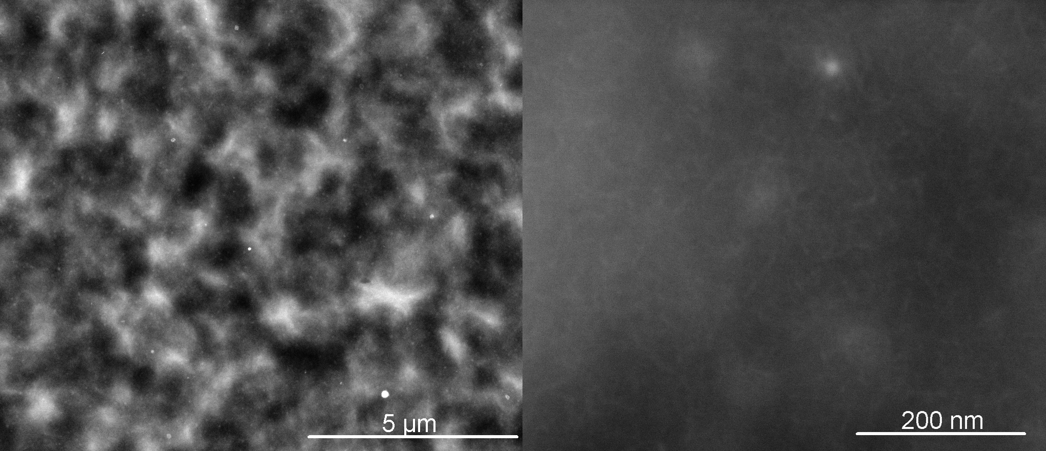
Um diese Probleme zu umgehen, verwenden wir verschiedene neue elektronenmikroskopische Techniken, wie die „low Energy scanning transmission electron microscopy“ (Low-keV-STEM) oder Phasenplatten-TEM um die Morphologie der Absorberfilme abzubilden. Die beiden unten stehenden Abbildungen zeigen zwei HAADF ("high-angle annular-dark field") STEM Abbildungen einer Absorberschicht, bestehend aus P3HT:PCBM. Bei den großskaligen Strukturen im linken Bild handelt es sich um Dickenvariationen in der Absorberschicht. Erst bei höherer Vergrößerung (rechtes Bild) ist die Nanomorphologie der Solarzelle in Form von kristallinen P3HT-Nadeln zu erkennen.
Selected conference poster presentations:
Selected Publications::
Organic Solar Cells:
[1] M. Pfaff, E. Müller, D. Gerthsen, M.F.G. Klein, A. Colsmann, U. Lemmer,
Low-energy electron transmission measurements of thin polymer films in a scanning electron microscope,
in W. Grogger, F. Hofer, P. Pölt (Eds.), Proc. MC2009 Microscopy Conference, Graz, Austria (2009),
Vol. 1: Materials Science, p. 215, Verlag der TU Graz 2009
[2] M. F. G. Klein, M. Pfaff, E. Müller, J. Czolk, M. Reinhard, S. Valouch, U. Lemmer, A. Colsmann and D. Gerthsen.
Poly(3-hexylselenophene) solar cells: Correlating the optoelectronic device performance and nanomorphology imaged by low-energy scanning Transmission electron microscopy.
Journal of Polymer Science Part B: Polymer Physics 50, 198-206 (2012)
[3] M. Pfaff, M. F. G. Klein, E. Müller, P. Müller, A. Colsmann, U. Lemmer and D. Gerthsen.
Nanomorphology of P3HT:PCBM-based absorber layers of organic solar cells after dierent processing conditions analyzed
by low-energy scanning transmission electron microscopy.
Microscopy & Microanalysis 18, 1380-1388 (2012)
[4] M. F. G. Klein, F. M. Pasker, S. Kowarik, D. Landerer, M. Pfaff, M. Isen, D. Gerthsen, U. Lemmer, S. Höger and A. Colsmann.
Carbazole-phenylbenzotriazole copolymers as absorber material in organic solar cells.
Macromolecules 46, 3870-3878 (2013).
[5] M. Pfaff, P. Müller, P. Bockstaller, E. Müller, J. Subbiah, W. W. H. Wong, M. F. G. Klein, W. Pisula, A. Kiersnowski,
S. R. Puniredd, W. Pisula, A. Colsmann,D. Gerthsen and D. J. Jones.
Bulk heterojunction nanomorphology of fluorenyl hexa-peri-hexabenzocoronene-fullerene blend lms.
ACS Applied Materials and Interfaces 5, 11554-11562 (2013)
Organische LED:
[1]S. Höfle, H. Do, E. Mankel, M. Pfaff, Z. Zhang, D. Bahro, W. Jaegermann, D. Gerthsen, C. Feldmann, U. Lemmer and A. Colsmann.
Molybdenum oxide anode buer layers for solution processed, blue phosphorescent small molecule organic light emitting diodes.
Organic Electronics 14, 1820-1824 (2013)
[2]S. Höfle, M. Pfaff, H. Do, C. Bernhard, D. Gerthsen, U. Lemmer and A. Colsmann.
Suppressing molecular aggregation in solution processed small molecule organic light emitting diodes.
Organic Electronics 15, 337–341 (2014)