
Superconducting Thin Films
In collaboration with the Institute of Technical Physics (ITEP), we investigate the microstructure of epitaxially grown thin films of application-relevant high-temperature superconductors such as REBa2Cu3O7-δ (REBCO for short, RE = rare-earth element such as Y, Gd, Er, ...) or Ba(Fe,Co)2As2. The latter belongs to the relatively young class of iron-based superconductors, which were only discovered in 2006. Electron microscopy provides insight into the atomic structure and chemical composition. The superconducting films are fabricated using different methods, such as pulsed laser deposition or chemical solution deposition, which affects the microstructure - and thus the superconducting properties. An important goal here is to increase the current-carrying capacity by selectively introducing non-superconducting defects or nanoparticles [1]-[3]. Magnetic flux lines can be pinned at such defects, leading to an improvement of the current-carrying capacity. By correlating microstructural studies with superconducting properties, we aim to get a better understanding of the fabrication processes of the films.
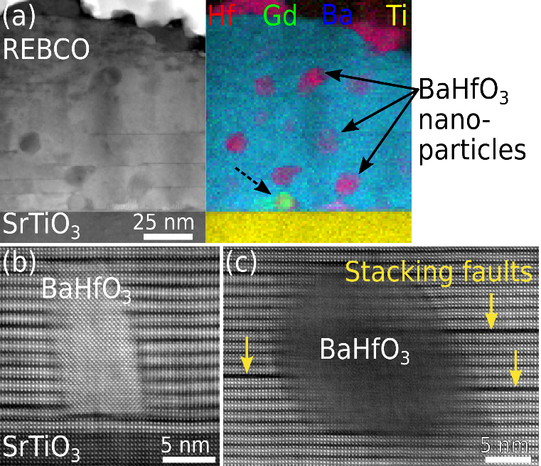
Scanning transmission electron microscopy (STEM) in combination with a high-angle annular dark-field (HAADF) detector is a commonly used imaging technique in materials science that allows a direct interpretation of the image contrasts. For example, the bright atomic columns in Figure 1b and c can be assigned to the heavy rare-earth elements and barium [1]. HAADF-STEM can be used to study the growth of the BaHfO3 nanoparticles shown here near the substrate (Fig. 1b, here SrTiO3) or in the superconducting layer (Fig. 1c). The crystal structure of the REBCO layer is disturbed by the BaHfO3 nanoparticles, which can lead to further defects such as the stacking faults marked with yellow arrows, which in turn can cause pinning. Spectroscopy using STEM allows chemical analysis of the BaHfO3 nanoparticles in the layer (Fig. 1a). The detected signals of some selected elements show their spatial distribution, e.g. Hf the position of the BaHfO3 nanoparticles. At the interface with the substrate, another precipitate can be seen, which contains a higher proportion of REs, here gadolinium (green, marked by the dashed arrow).
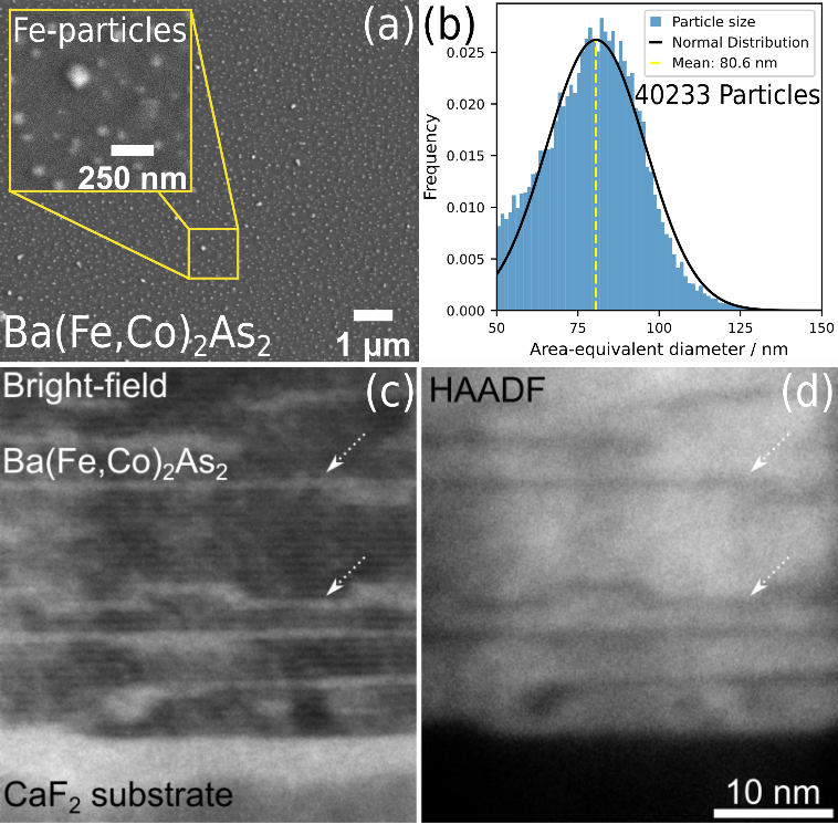
In addition to material analysis in the TEM, we also apply structural analysis in the scanning electron microscope (SEM) [4]. Here, the surface structure can be studied, e.g., iron-rich precipitates in Ba(Fe,Co)2As2 [5], [6] (Fig. 2a). Using machine learning methods, many thousands of particles can be automatically segmented and measured from such SEM images and the particle sizes evaluated [5] (Fig. 2b). In addition to conventional surface imaging, modern SEMs can also be operated in STEM mode for electron-transparent samples (so-called STEM-in-SEM). In addition, a focused ion beam in the same instrument (FIB/SEM system) can be used for sample preparation. This combination allows sample preparation and STEM imaging in one instrument. This is especially advantageous for reactive materials, as the sample remains in the vacuum of the FIB/SEM system. For Ba(Fe,Co)2As2, for example, oxidation of planar defects could be avoided [5] (Fig. 2c and d).
Literature
[1] L. Grünewald, P. Cayado, J. Hänisch, B. Holzapfel, and D. Gerthsen, “Structural and chemical properties of superconducting rare-earth barium copper oxide/BaHfO3 nanocomposites with rare-earth mixtures,” Microscopy and Microanalysis, vol. 27, no. S1, pp. 2876–2879, Aug. 2021, doi: 10.1017/S1431927621010023.
[2] S. Meyer, M. Langer, L. Grünewald, J. Hänisch, D. Gerthsen, and B. Holzapfel, “Pulsed Laser Deposition of quasi-multilayer superconducting Ba(Fe0.92Co 0.08 ) 2 As 2 -BaHfO 3 nanocomposite films,” Journal of Physics: Conference Series, vol. 1559, no. 1, p. 012052, Jun. 2020, doi: 10.1088/1742-6596/1559/1/012052.
[3] S. Meyer, “Introduction of quasi-multilayer pulsed laser deposition for enhanced superconducting properties of Ba(Fe$_{0.92}$Co$_{0.08}$)$_2$As$_2$ thin films,” Karlsruhe Institute of Technology (KIT), 2021. doi: 10.5445/IR/1000127915.
[4] L. Grünewald et al., “Analysis of superconducting thin films in a modern FIB/SEM dual-beam instrument,” Microscopy and Microanalysis, vol. 27, no. S1, pp. 1056–1058, Aug. 2021, doi: 10.1017/S1431927621003986.
[5] L. Grünewald et al., “Structural and chemical properties of superconducting Co-doped BaFe2As2 thin films grown on CaF2,” Supercond. Sci. Technol., vol. 34, no. 3, p. 035005, Jan. 2021, doi: 10.1088/1361-6668/abcecf.
[6] M. Langer et al., “On the growth of Co-doped BaFe2As2 thin films on CaF2,” Journal of Physics: Conference Series, vol. 1293, no. 1, p. 012014, 2019, doi: 10.1088/1742-6596/1293/1/012014.