
Scanning electron microscopy (SEM)
Scanning electron microscopy (SEM) is used to study the surface structure of samples in materials research, nanotechnology, solid state physics, chemistry, process engineering, biology and geology. In most cases, no complex sample preparation is required. Electrically insulating objects must be vapor deposited with a thin carbon, gold or platinum film to avoid charging the sample in the microscope. Biological objects often need to be dried before examination.
The SEM is characterized by the following features:
- high resolution when imaging with secondary electrons: structural details down to 1 nm (for electrically conductive samples)
- chemically sensitive imaging (qualitative) with backscattered electrons
- high depth of field
- combination of topography and elemental distribution by energy dispersive X-ray spectroscopy (EDXS) in scanning electron microscope
Typical applications of SEM are:
- Investigation of fracture surfaces and wear phenomena on surfaces
- Investigation of surface coatings
- Analysis of particles and precipitates (size, number, density, chemical composition)
- Analysis of material inhomogeneities
- Process control, process improvement, incoming and qualitiy control
Contact
Applications as well as the fee schedule for services can be found here.
Examples for the use of scanning electron microscopy
ZnO nanopillars
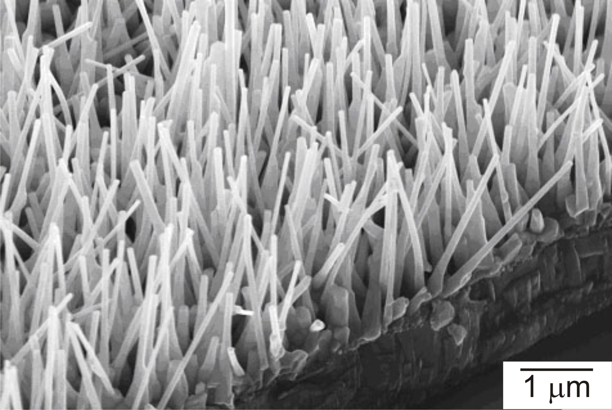
Sample from the group of Prof. Dr. H. Kalt, Institute for Applied Physics, Karlsrueh Institute of Technology (KIT)/University of Karlsruhe
After critical point drying, biological objects can also be examined with the SEM. As an example, an HT-29 intestinal carcinoma cell is hown in fugre (a). The image with secondary electrons (a) shows the sruface topography, while the image of the same cekk with backscattered electrons (b) is chemically sensitive. The bright areas marked with arrows indicate Pt patricles located at hte cell surface. The internal structure of a an HT-29 cell can be imaged after "milling" with a focused Ga+ ion beam in a combined FIB (Focused-Ion-Beam)/SEM system (Figure (c) left). Figure (d) shows EDXS spectra of an approximately 30nm small Pt particle and the adjacent cemm matrix withou Pt signal.
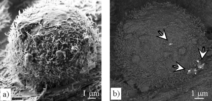
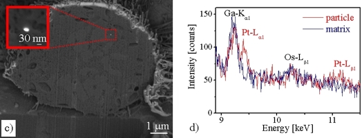
J. Pelka et al., "Cellular Uptake of Platinum Nanoparticles in Human Colon Carcinoma Cells and Their Impact on Cellular Redox Systems and DNA Integrity, Chem. Res. in Toxicology 22, 649 (2009)
"Large" object imaged with high depth of field: Microzawheel with shaft
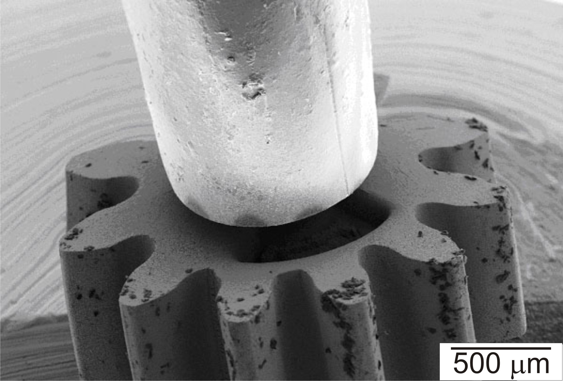
Sample: Dr. B. Okolo, Prof. Dr. A. Wanner, Institute of Materials Science I, Karlsrueh Institute of Technology (KIT)/University Karlsruhe
Fracture surface of a C/C (carbon matrix/carbon fiber) composite material
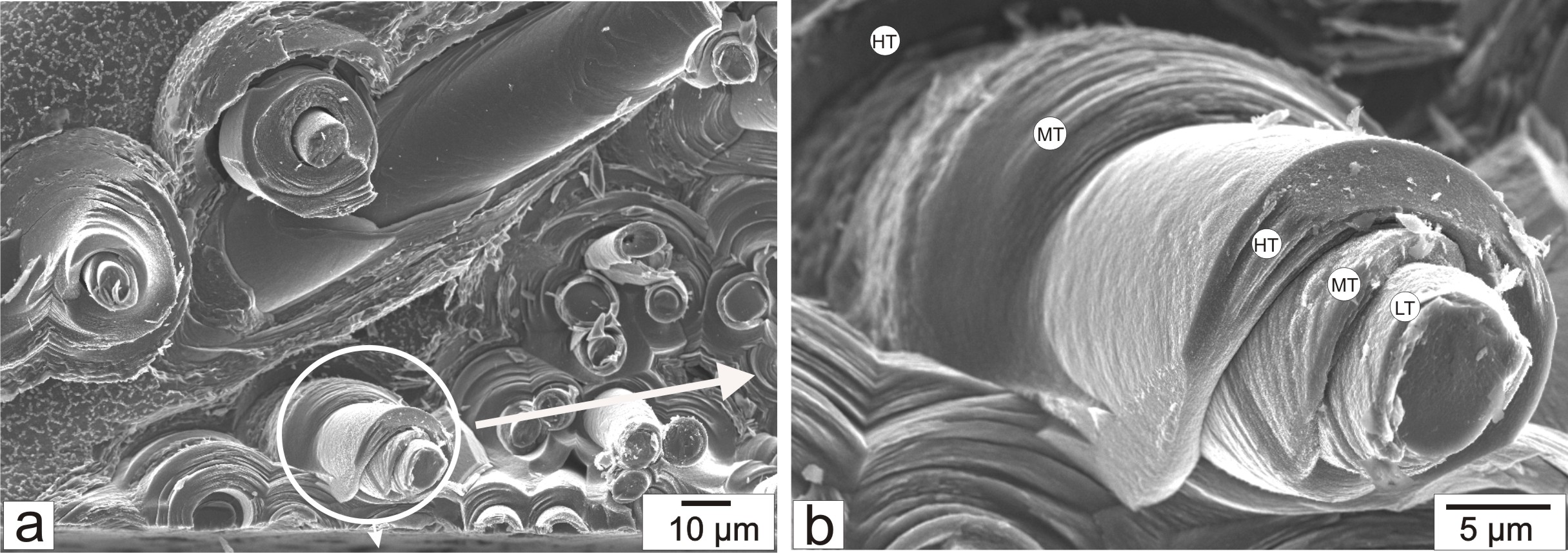
B. Reznik, D. Gerthsen, "Microscopic Study of Failure Mechanisms in Infiltrated Carbon Fiber Felts", Carbon 41, 57 (2003)
Bacteria
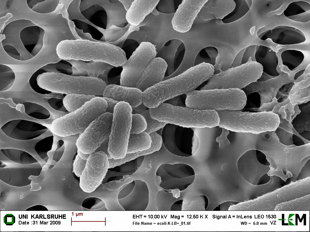
Scanning electron microscopy image of E. coli DSM 1103. The cells were dropped and prepared on membrane filter by Mareike Hartmann for Diploma work, KIT, Institute of Organic Chemistry, Department Biochemistry.