Welcome
We were pleased to welcome Prof. Michael Titus from Purdue University, a long-time colleague and friend of our group. His visit provided an excellent opportunity for valuable scientific exchange and inspiring discussions. Thank you for visiting LEM!
International Guest: Prof. Tresa Pollock
We were honored to welcome Prof. Tresa Pollock from UC Santa Barbara, USA, as our guest at LEM.
The exchange and discussions were truly enriching, and we look forward to welcoming you again soon!
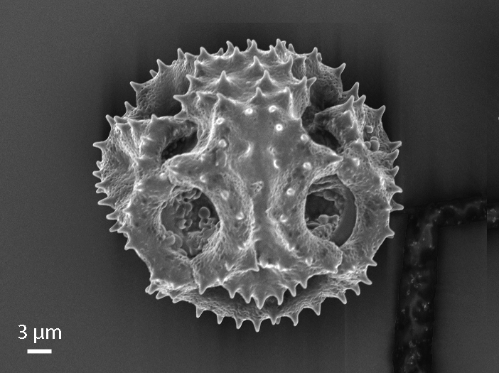
On Girls' Day, the LEM received a visit from four pupils. They prepared their own samples and examined these using light microscopy and SEM, being able to capture their very own stunning images (see image: dandelion pollen). We all greatly enjoyed presenting our work and exploring the fascinating structures. We were especially pleased by the many curious questions about microscopy and research here at KIT.

We congratulate Hemanth Thota on successfully defending his PhD thesis—a fantastic achievement. Well done! 🎉

We warmly welcome Judith Burger to the LEM team! She joins us as a Team Assistant, and we wish her a fantastic start with us.
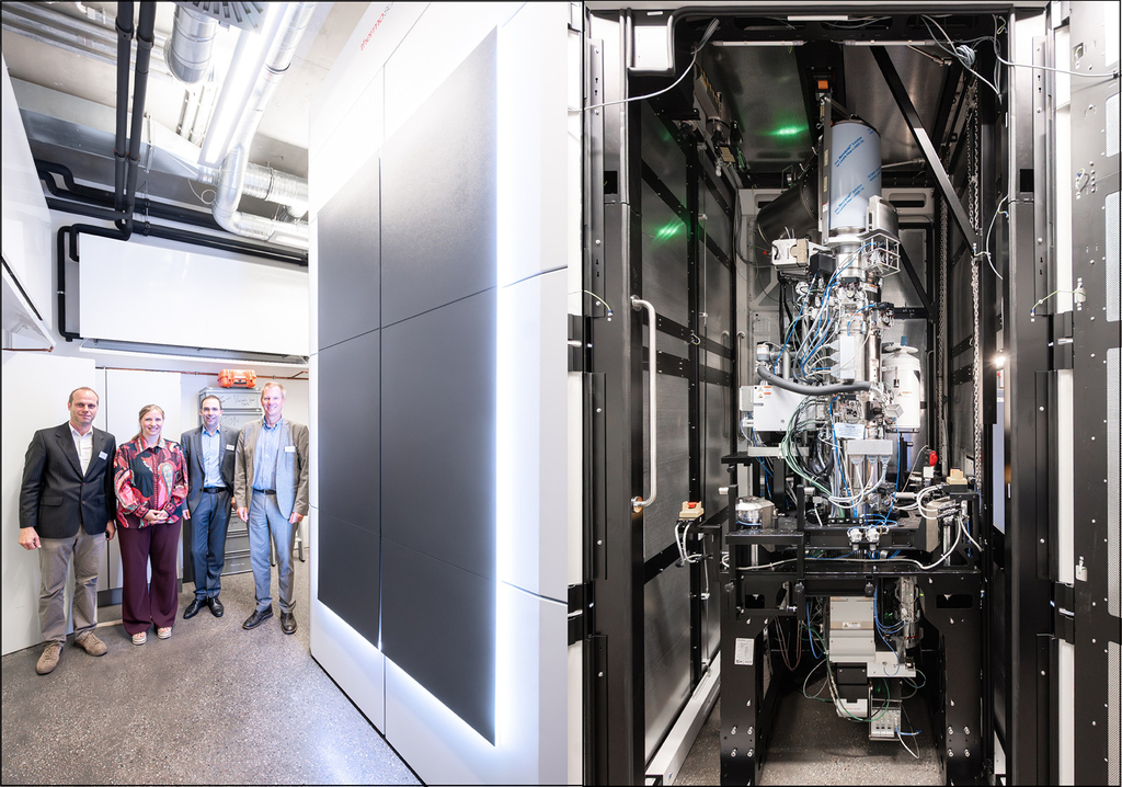
Our new Spectra Ultra is up and running since March! With its impressive ease of use, we’re already capturing atomic-scale images faster than ever.

We are excited to welcome Victoria Tucker to LEM as an Alexander von Humboldt Fellow. Great to have you on board!

We are delighted to welcome Mareike Dortmund to LEM as a new PhD student working on electron microscopy of materials under extreme conditions. We wish you a fantastic and successful PhD journey—great to have you on board!